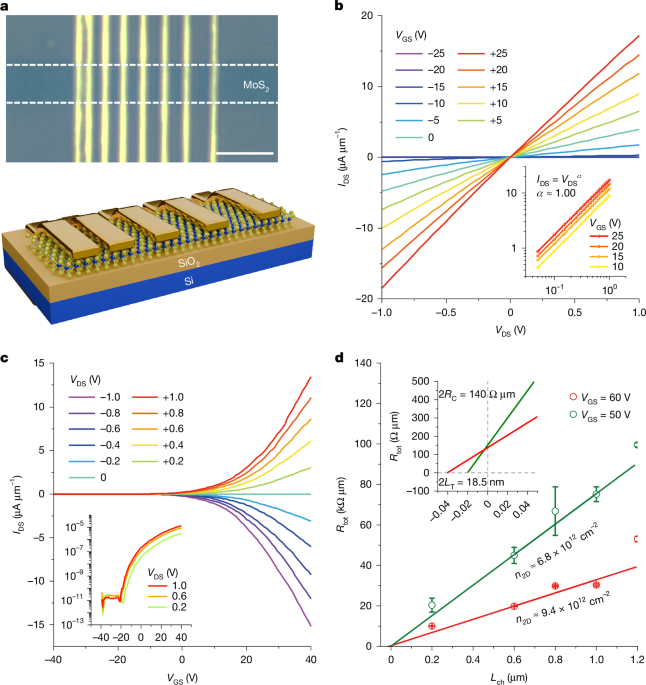
Cross-sectional scanning tunnelling microscopy shows a 2 nm carrier transfer length in bismuth-contacted monolayer MoS2 transistors, defining metal-contact scaling limits for sub-10 nm 2D electronic devices.
In response to the increasing needs of artificial intelligence computations and rising requirements in data centres and mobile devices, the necessity to fabricate transistors that are high-density, h… [+30745 chars]